Henri Jaffres
Scientific Research National Center (CNRS), France
Title: Electrical spin injection and detection in molybdenum disulfide multilayer channel
Biography
Biography: Henri Jaffres
Abstract
Molybdenum disulfide has recently emerged as a promising two- dimensional semiconducting material for nano-electronic and spintronic applications. However, the demonstration of an electron spin transport through ferromagnetic source and drain connecting a semiconducting MoS2 channel remains challenging. Here, the author will present the experimental evidence of the electrical spin-injection and spin-detection in the conduction band of a multilayer MoS2 semiconducting channel using a two terminal spin-valve configuration geometry. A magnetoresistance around 1% have been observed through a 450 nm long, 6 monolayer thick MoS2 channel with a Co/MgO tunneling spin injector and detector. It is found that keeping a good balance between the interface resistance and channel resistance is mandatory for the observation of the two-terminal magnetoresistance. Moreover, the electron spin-relaxation is found to be greatly suppressed in the multilayer MoS2 channel with an in-plane magnetization and spin-polarization. The long spin-diffusion length (approximately 235 nm) could open a new avenue for spintronic applications using multilayer transition metal dichalcogenides. In this talk, corollary to experiments, I will particularly emphasize on the mechanism of spin-injection at interfaces between a spin-polarized tunnel junction and a semiconductor channel, homogeneous or not. The latter can be composed of several regions, uniformly doped or depleted to form a Schottky contact and possibly location of a conduction made by hopping. I will extend the conditions for spin-injection from a spin- polarized ferromagnetic source into a Schottky contact on the ground of the experiments observed with success on MoS2 systems.

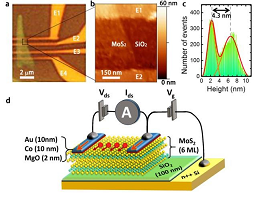
Figure 1: Multilayer MoS2-based lateral spin-valve device. (a) Optical image of the device with the multilayer MoS2 flake on 100 nm SiO2/Si(nþ þ) substrate, the E1, E2, E3 and E4 indicate the four Au/Co/MgO electrodes. (b, c) AFM measurement (in tapping mode) focused on the MoS2 channel between E1 and E2 electrodes. The thickness of MoS2 is determined by the Gaussian distribution of pixel height in the square region in b. (d) Schematics of the lateral spin-valve device. The multilayer MoS2 serves as a spin transport channel, and two Au/Co/MgO electrodes are used to inject spin (Vds) and measure the current (Ids). A back-gate voltage (Vg) between the substrate and one top contact is used to modulate the carrier density in MoS2.
Recent Publications:
1.A Fert, J M George, H Jaffrès, R Mattana (2007) Title. IEEE transactions on electron devices 54:5.
2.A Fert, H Jaffrès (2001) Title. Phys. Rev. B 64:184420.
3.M Tran, H Jaffrès, C Deranlot, J M George, A Fert, A Miard, A Lemaître (2009) Title. Phys. Rev. Lett. 102: 036601.


