


Biography
Biography: Sezai Elagoz
Abstract
InGaAs/InAlAs superlattices (SLs) are very attractive and suitable for QCL applications due to the availability of lattice matching on InP substrate and large conduction band offset. When InxGa1-xAs and InyAl1-yAs compounds are lattice matched to InP substrate, this allows fabricating QCL devices with an emission wavelength at λ>4µm. Similarly, to go larger wavelengths, the same materials can be used by utilizing a technique known as strain-balancing to overcome the difficulties arise from lattice mismatch. Precise thickness control, alloy composition control and repeatability of the SLs are the most critical issues to be dealt with in growth studies to obtain the desired device structures. The thinnest layer thickness is a few monolayers and the device performance is quite sensitive to interface roughness. Molecular beam epitaxy (MBE) is the generally preferred growth technique due to the requirement of having very thin layers with sharp interfaces. However, QCL also includes thick layers such as claddings for which MOCVD suits the best. For these reasons, it is worth efforts to find a way to grow the whole structure via MOCVD. Using special growth conditions and smaller mass flow controllers (MFCs) it is possible to precisely control the gas flow quantity dilution and injection of metalorganic sources. Transmission Electron Microscope (TEM), Scanning Tunneling Electron Microscope (STEM) and similar techniques are widely used to determine the exact thickness of epitaxially grown SLs. However, these techniques are destructive, relatively expensive, time consuming and require an elevated level of expertise for the sample preparations as well as the sample measurement. The high-resolution x-ray diffraction is a non-destructive, economic, quick and robust technique than electron microscopes and depending on the scan type it is quite sensitive to thickness change, alloy composition and interface quality and, as we demonstrate, it can be used to find the thicknesses for very thin layers.
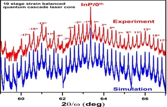
Figure-1 10 stage strain balanced QCL structure grown by MOCVD
Recent Publications
1. Demir I, Elagoz S (2017) V/III ratio effects on doping of high quality InAlAs for Quantum Cascade Laser structures. Superlattices and Microstructures 104:140-148.
2. Demir I, Robin Y, McClintock R, Elagoz S, Zekentes K, Razeghi M, (2017) Direct growth of thick AlN layers on nanopatterned Si substrates by cantilever epitaxy. Physica Status Solidi (a) 214 (4): 1600363.
3. Demir I, Elagoz S (2016) Interruption time effects on InGaAs/InAlAs superlattices of quantum cascade laser structures grown by MOCVD. Superlattices and Microstructures 100:723-729.
4. Demir I, Elagoz S (2016) Growth of InGaAs/InAlAs superlattices by MOCVD and precise thickness determination via HRXRD. Gazi University Journal of Science 29(4):947-951.
5. Tansel T, Hostut M, Elagoz S, Kilic A, Ergun Y, Aydinli A (2016) Demir I, Elagoz S (2016) Electrical performance of InAs/AlSb/GaSb superlattice photodetectors. Superlattices and Microstructures 91:1-7.