


Maryam Alimoradi Jazi
University of Utrecht, Netherlands
Title: Transport properties of a two-dimensional PbSe square superstructure in an electrolytegated transistor
Biography
Biography: Maryam Alimoradi Jazi
Abstract
Colloidal semiconductor nanocrystals have gained interest because their optical and electronic properties can be tuned by varying shape, size and composition. Recently, 2D square and honeycomb superstructure of lead- and cadmium-chalcogenide quantum dots (QDs) have been prepared. These superstructures are formed by assembling PbSe nanocrystals in a monolayer at the toluene suspension air/interface after which the nanocrystals attach via their four vertical {100} facets [1],[2]. Theoretical studies show that these 2-D systems have profoundly distinct band structures compared to other continious nanosheets with the appearance of Dirac cones in the case of the honeycomb [3],[4]. Strong electronic coupling via the atomic connections of the QDs in the superstructure may result in a higer mobility compared to the self-assembled lead chalcogenide QDs that are less strongly coupled due to the (in)organic ligands [5].
In our research, we use electrolyte-gated transistors (Figure 1a) to study the optoelectronic properties and transport characteristics of 2-D PbSe superstructures [6]. The potential of the gate electrode determines the Fermi level with respect to the conduction band (CB) or valance band (VB) of the superstructure. First, to monitor the stability of the superlattice under electron injection we measure the differential capacitance as a function of gate voltage. From the total injected charge and an estimation of the number of nanocrystal sites in the gated part of the PbSe superlattice we calculate charge density of the superstructure. Second, the conductivity of the network is measured as a function of the Fermi level position. Finally, the mobility of the system is calculated from conductivity and charge density. As an alternative methode to quantify electron injection into the PbSe superlattice, the optical absorbsion measurent is done while sweeping the potential. Furthermore, actual position of the Fermi level can also be obtained by measuring the inter-band light absorption quenching which monitors the precise occupation of the bands (Figure1b). In our recent work, we report the first study of electron transport in a 2-D system with a square geometry in which band occupation is assured by the high electron denity of 8 electron per nanocrystal site.The electron mobility between 5 and 18 cm2/Vs is observed for these supersructures [7].
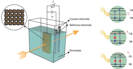
Figure. 1 a) electrolyte gated transistor, b) Interband light absorption quenching
Recent Publications
1. W.H. Evers et al., Nano Lett., 13, 2317-2323 (2013).
2. M.P. Boneschanscher et al., Science, 344, 1377 (2014).
3. E. Kalesaki et al., Phys. Rev. X 4, 011010 (2014).
4. E. Kalesaki et al., Phys. Rev. B 88, 115431 (2013).
5. W.H. Evers et al., Nature Communications 6, 8195 (2015).
6. D. Vanmaekelbergh et al., Electrochemica Acta, 53, 1140-1149 (2007).
7. M.Alimoradi Jazi et al., Nano Lett., 17, 5238-5243 (2017)