Takumi Namba
Tokyo University of Science, Japan
Title: MSE-07: Preparation of oxide semiconductors thin films for the transparent electrode by helicon-wave excited plasma sputtering method
Biography
Biography: Takumi Namba
Abstract
Silicon (Si)-based solar cells have a market share of more than 90%, and are expanding in this market. However, high purity Si is very expensive and would be the risks of short supply and price fluctuation. Recently, Cu(Inï½¥Ga)Se2(CIGS) based thin film solar cells have been attracted as high conversion efficiency as a high efficiency thin film solar cell of the next generation and achieved the highest conversion efficiency of 20% over. The top electrode material for CICS based solar cell is widely used ZnO:Al and is required to be low resistivity (under 10-3 Ωcm) and optical transparency (larger than 80% in transmittance). Moreover, the preparation of good crystallinity ZnO:Al thin films is expected for improvement of the conversion efficiency of CIGS based solar cells.

In this study, we tried to prepare ZnO:Al thin films with good crystallinity by helicon wave excited magnetron sputtering method and aimed to establish conditions for preparation. ZnO:Al thin films prepared by this method were evaluated for crystallinity, optical transmittance, and thickness by X-ray diffraction (XRD), recording spectrophotometer, and stylus surface profiler.
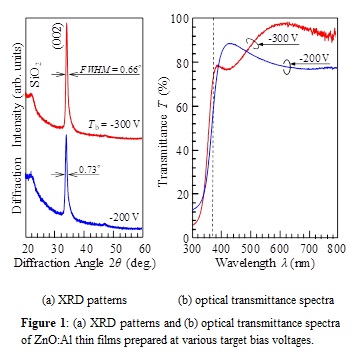
Figure1 shows (a) XRD patterns and (b)optical transmittance spectra of ZnO:Al thin films prepared at various the target bias voltages. RF power, substrate temperature, and deposition time were 400 W, 200 ℃, and 3 hours, respectively. ZnO:Al thin film prepared at -300 V exhibited the wurtzite structure (α-ZnO), optical absorption edge of 360 nm (3.37 eV) and good optical transparency
